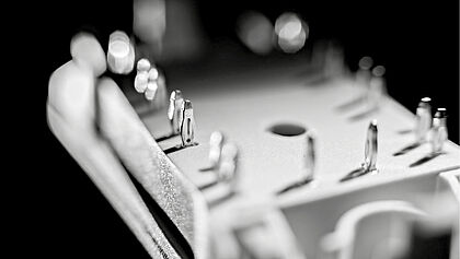
Vincotech的压接技术大大降低了PCB组装时间和工作量。 在汽车工业中获得成熟应用的压接引脚使得无需焊接、切割加工时间和成本,提高了生产产能。 无需焊接模块,工程师在设计上享有极大的灵活性。 模块可以轻松地安装在PCB的顶部或底部,无需额外的成本和工作。
特性
- 批准的圆形压接区域
- 符合DIN和IEC标准
- 锥形引脚针头
- 几乎适用于所有封装
- Application Note: Vincotech's Press-fit Pin
- Video: Press-fit technology - the new interconnection technology
- Video: Press-in process with flow 1B housing
Press-fit pin
Press-fit pins forge a solid bond between two parts that requires no additional soldering. Frictional force holds the parts together after they have been joined to create a gas-tight, cold-welded, solder-less connection.
Press-fit pins emerged in the early 1970s. The DIN 41611-5 standard for this technology was first published in 1984, and the IEC guidance 60352-5, "Solder-less connections – Part 5: Press-in connections – General requirements, test methods and practical guidance,” soon followed. Components that meet these qualifications are called 'compliant,' and the term 'compliant pin' is widely used throughout the market.
Engineers started replacing soldered pins and screws with these alternatives in the mid-1980s, and modules equipped with these pins debuted in 2005.
Today these pins come in various sizes and shapes, one of the most common being the eye-of-the-needle, or Press-fit, pin. Its ability to stand up to vibrations prompted automakers to use it for diesel engines.
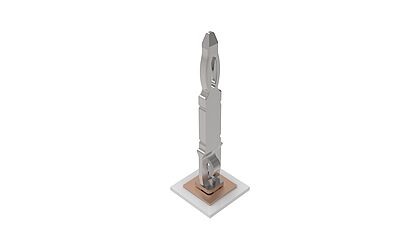
Figure 1 shows an improved eye-of-the-needle Press fit pin which was patented and has been used in Vincotech modules since 2008. Follow the links to learn more about European, German and US patents.

The pin is made of a copper alloy with nickel plating and a tin finish. Every Vincotech pin comes with an s-bend at the bottom to provide stress relief. It facilitates assembly and may be pushed or pulled as needed for a pre-bent DCB or baseplate. This stress-relief also offsets heat- and cold-induced expansion and contraction.
|
Property |
Value |
Unit |
|---|---|---|
|
Underplating |
Ni |
|
|
Surface of pin |
Tin |
|
|
Recommended PCB finish |
I-Sn |
|
|
Alternative PCB finish |
HA(S)L / NiAg |
|
|
Current carrying capability @ ∆T = 25 K |
30* |
A |
|
Thermal conductivity λ |
320 |
W/mK |
|
Thermal capacity c |
381 |
J/kgK |
|
Thermal expansion coefficient α |
17.6 |
1-06/K |
|
Density ρ |
8.92 |
g/cm³ |
* Depending on PCB layout

